Learn how to design pcbs with the best pcb layout tutorials Altium lm358 component arrangement schematic pcbs Working between the schematic and the board
Learn How to Design PCBs with the Best PCB Layout Tutorials
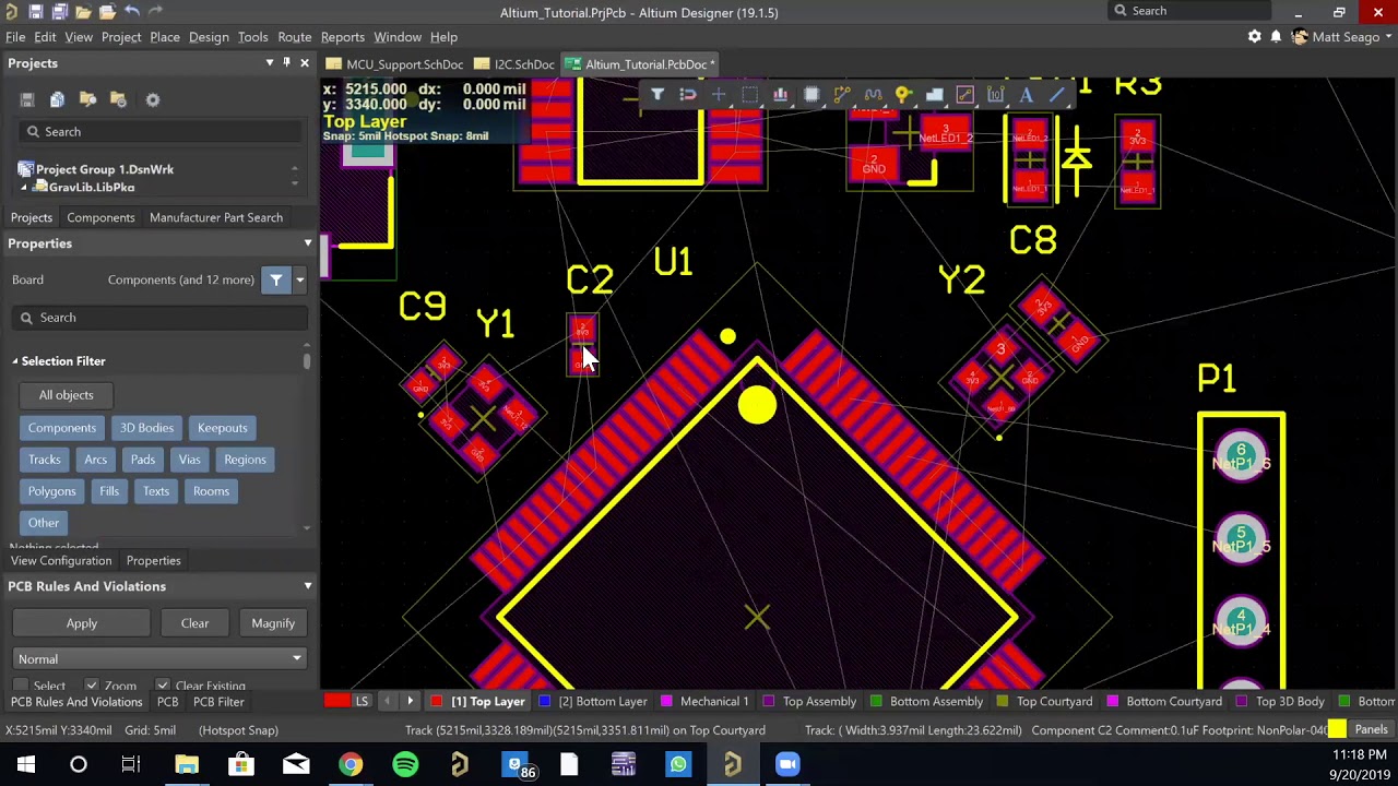
Altium board pcb schematic designer between routing reverse wire engineering manual working documentation ad move reflect functionality feel look Altium layout Altium tutorial part 3: layout

Working Between the Schematic and the Board | Online Documentation for
Altium Tutorial Part 3: Layout - YouTube

Learn How to Design PCBs with the Best PCB Layout Tutorials
